Today, only a little bit of breadboarding and some maths ...
While browsing the web to try to learn about oscillators, I found this cool circuit:
While browsing the web to try to learn about oscillators, I found this cool circuit:

I built it in LTSpice and the simulation says vOut is supposed to do this:

It not a perfect sine wave, but it's quite close, and LTSpice predicts it should oscillate at around 136 Hz:

Something nice about this circuit is that needs only 4 resistors, 3 caps and an 1 NPN BJT transistor.
In particular this oscillator does not need any inductors (inductors are bulky, expensive and prone to EM noise).
So, let's build this circuit on the breadboard and check what happens:

As you can see on the pic, it is quick and easy to put together.
Let's power it up, hook up the 2N2222 collector to the scope to see what voltage at vOut looks like:

So the real world voltage for this circuit looks very much like what LTSpice predicted.
In particular, the scope curve has the exact same little bump at the botttom left of the sine wave as the one in the simulation.
Scope also says oscillation frequency is stable, at around 140.8Hz. This is not too far off what the frequency LTSpice predicted (the components I used to build it aren't precision, so no surprise if predicted frequencies and actual aren't exactly equal).
In particular, the scope curve has the exact same little bump at the botttom left of the sine wave as the one in the simulation.
Now, I am trying to understand why it oscillates, and that is not exactly intuitively obvious.
I'm attacking this is by looking at the 2N2222 NPN.
The transistor basically acts like a valve that controls the amount of current flowing from its collector to its emitter.
Current is pushed by a constant voltage source through a 1k resistor down into the collector of the transistor , and the current coming out of the emitter of the transistor goes directly to ground.
Current is pushed by a constant voltage source through a 1k resistor down into the collector of the transistor , and the current coming out of the emitter of the transistor goes directly to ground.
Basic property of BJT transistors: the amount of current flowing from collector to emitter is in turn more or less proportional to the signal applied to the transistor base.
In this circuit, that signal happens to be taken from the collector voltage itself, first piped through a "feedback network" and injected into the transistor base.
So, the magic clearly happens in the feedback network.
Let's take a closer look at what that looks like:
Let's take a closer look at what that looks like:
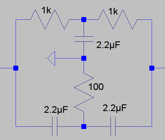
After some quality time with Google and the help of a kind soul at electronics.stackexchange.com, I found out that this sub-circuit is called a "Twin-T filter" because it looks like two "T" shaped filters (at top and bottom) combined into a large filter.
The Twin-T filter (wikipedia) is a so-called "notch filter": it lets almost all frequencies through, with the exception of a small band of frequencies that get strongly attenuated (the frequencies within the "notch", hence the name).
To intuitively understand how the notch filter works, you have to look at it as two simple T-shaped filters connected in parallel.
The top part (the top "T") with the two 1k resistors and the 2.2μF is a low-pass filter:
- At high frequencies, the vertical cap conducts and dumps everything to ground. High frequencies therefore do not make it through the filter.
- On the other hand, at low frequency the vertical cap is highly resistive and these frequencies pass through the horizontal resistors.
The bottom part with the two 2.2μF is a high-pass filter:
- At high frequencies, the horizontal caps conduct and allow most of the signal to make it through safe a little bit that dumps to ground through the 100Ω resistor.
- At low frequency the two horizontal caps are highly resistive and nothing makes it through.
Since these two filters are connected in parallel, they behave as a logical "OR":
- low frequencies pass almost unhindered through the top part
- high frequencies pass almost unhindered through the bottom part
- a small subset of frequencies is neither making it through the top nor the bottom.
One way to verify this intuition is to ask LTSpice to run an AC analysis of that specific portion of the circuit.
Lo and behold, we see the notch clearly: the filter does indeed drop only frequencies in a narrow band around 140Hz:

The graph above is a "Bode Plot" : it has
Both attenuation (left Y axis) and frequencies (X axis) have a logarithmic scale.
- frequencies on the X axis
- signal amplitude attenuation on the left Y axis (the V-shaped curve)
- "phase shift" on the right Y axis (the S-shaped curve).
Both attenuation (left Y axis) and frequencies (X axis) have a logarithmic scale.
What we notice is that frequencies which are filtered out (attenuated) the strongest are also "phase-shifted", or "delayed" the most, with the maximum shift (180 degrees) more or less aligned with the tip of the notch, where the attenuation is also maximum.
It turns out - and a tad counter-intuitively so - that the frequency that is maximally attenuated is the one and only frequency that will eventually "remain" in the collector->emitter branch of the circuit.
Go figure ...
The explanations I've read so far is that it is because that specific frequency is the most shifted/delayed (hence the name "phase-shift oscillator"), but to be honest, I'm still trying to wrap my head around this one from an intuitive point of view.
Go figure ...
The explanations I've read so far is that it is because that specific frequency is the most shifted/delayed (hence the name "phase-shift oscillator"), but to be honest, I'm still trying to wrap my head around this one from an intuitive point of view.
Let's shift gear and look at the math: time to pull out Mathematica and dig a little deeper.
To understand the Twin-T filter, we model the topology with completely general impedances and we perform a full nodal analysis:
$z_{ij}$ denotes impedances from node $i$ to node $j$
$i_{ij}$ denotes currents from node $i$ to node $j$
$v_{i}$ denotes voltage between node and ground $i$
Twin T filter : H topology with grounded center:
================================================
Voltage Source
is0 vs vg i2g
+----------<----------+ +----------<----------+
| |
| i01 i01 v1 i12 i12 ^
| +---->---z01--->---+--->---z12--->----+ |
| | | | |
is0 V | i14 v | z2g (load)
| | | | |
| ^ i01 z14 i12 v |
| | | | ^
| | i14 v | |
| | | i4g | |
+-->--+ v0 v4 +--->---+ vg v2 +-->--+
is0 | | | i2g
| v i43 |
| | |
i03 v z43 ^ i32
| | |
| v i43 |
| | |
+---->---z03--->---+--->---z32--->----+
i03 i03 v3 i32 i32
Step 0 : dumb, brute force application of the nodal analysis method gives us 16 equations:
Step 1 : get rid of the 7 obvious current variables using equations from the Ohm's law section:
\[\left( \begin{array}{c} \text{vg}=0 \\ \text{v0}=\text{vs} \\ \text{v4}=\text{vg} \\ \text{i4g}+\frac{\text{v2}-\text{vg}}{\text{z2g}}=\text{is0} \\ \text{is0}+\frac{\text{v1}-\text{v0}}{\text{z01}}+\frac{\text{v3}-\text{v0}}{\text{z03}}=0 \\ \frac{\text{v0}-\text{v1}}{\text{z01}}+\frac{\text{v2}-\text{v1}}{\text{z12}}+\frac{\text{v4}-\text{v1}}{\text{z14}}=0 \\ \frac{\text{v1}-\text{v2}}{\text{z12}}+\frac{\text{v3}-\text{v2}}{\text{z32}}+\frac{\text{vg}-\text{v2}}{\text{z2g}}=0 \\ \frac{\text{v0}-\text{v3}}{\text{z03}}+\frac{\text{v2}-\text{v3}}{\text{z32}}+\frac{\text{v4}-\text{v3}}{\text{z43}}=0 \\ \frac{\text{v1}-\text{v4}}{\text{z14}}+\frac{\text{v3}-\text{v4}}{\text{z43}}=\text{i4g} \\ \end{array} \right) \]
Step 2 : get rid of the 3 obvious voltage variables using equations from the constant voltage section:
\[ \left( \begin{array}{c} \text{i4g}+\frac{\text{v2}}{\text{z2g}}=\text{is0} \\ \text{is0}+\frac{\text{v1}-\text{vs}}{\text{z01}}+\frac{\text{v3}-\text{vs}}{\text{z03}}=0 \\ \text{v1} \left(\frac{1}{\text{z01}}+\frac{1}{\text{z12}}+\frac{1}{\text{z14}}\right)=\frac{\text{v2}}{\text{z12}}+\frac{\text{vs}}{\text{z01}} \\ \frac{\text{v1}-\text{v2}}{\text{z12}}+\frac{\text{v3}-\text{v2}}{\text{z32}}=\frac{\text{v2}}{\text{z2g}} \\ \text{v3} \left(\frac{1}{\text{z03}}+\frac{1}{\text{z32}}+\frac{1}{\text{z43}}\right)=\frac{\text{v2}}{\text{z32}}+\frac{\text{vs}}{\text{z03}} \\ \text{i4g}=\frac{\text{v1}}{\text{z14}}+\frac{\text{v3}}{\text{z43}} \\ \end{array} \right) \]
Step 3 : with a little more work, eliminate $v1, v3, is0, i4g$ leaves us with two equations:
\[
\left(
\begin{array}{c}
\text{v2} \left(\frac{\text{z01}+\text{z14}}{\text{z01} (\text{z12}+\text{z14})+\text{z12} \text{z14}}+\frac{\text{z03} (\text{z2g}+\text{z32}+\text{z43})+\text{z43} (\text{z2g}+\text{z32})}{\text{z03} \text{z2g}
(\text{z32}+\text{z43})+\text{z2g} \text{z32} \text{z43}}\right)+\text{vs} \left(-\frac{\text{z14}}{\text{z01} (\text{z12}+\text{z14})+\text{z12} \text{z14}}-\frac{\text{z43}}{\text{z03}
(\text{z32}+\text{z43})+\text{z32} \text{z43}}\right)=0 \\
\frac{-\text{v2} \text{z43} (\text{z01} (\text{z03}+\text{z12}+\text{z14}+\text{z32})+\text{z14} (\text{z03}+\text{z12}+\text{z32}))-\text{v2} \text{z03} (\text{z01} (\text{z12}+\text{z14}+\text{z32})+\text{z14}
(\text{z12}+\text{z32}))+\text{vs} \text{z43} (\text{z01} (\text{z12}+\text{z14})+\text{z14} (\text{z03}+\text{z12}+\text{z32}))+\text{vs} \text{z03} \text{z14} \text{z32}}{(\text{z01} (\text{z12}+\text{z14})+\text{z12}
\text{z14}) (\text{z03} (\text{z32}+\text{z43})+\text{z32} \text{z43})}=\frac{\text{v2}}{\text{z2g}} \\
\end{array}
\right)
\]
Even if it isn't obvious at first glance, it turns out that last two equations are in fact equivalent and Mathematica confirms it ... we probably introduced a redundant equation somewhere in the initial mix, no biggie. As long as they are equivalent and don't produce a contradiction, we can just user either of the two.
We pick the first one and ask Mathematica to solve for $v2$:
\[
\text{v2}=vs\times
\frac{\text{z2g}.(\text{z14}.\text{z43}.(\text{z01}+\text{z03}+\text{z12}+\text{z32})+\text{z01}.\text{z12}.\text{z43}+\text{z03}.\text{z14}.\text{z32})}{\text{z01}.\text{z43}.(\text{z03}.(\text{z12}+\text{z14}+\text{z2g})+\text{z32}.(\text{z12}+\text{z14}+\text{z2g})+\text{z2g}.(\text{z12}+\text{z14}))+\text{z01}.\text{z03}.(\text{z32}.(\text{z12}+\text{z14}+\text{z2g})+\text{z2g}.(\text{z12}+\text{z14}))+\text{z14}.\text{z43}.(\text{z03}.(\text{z12}+\text{z2g})+\text{z32}.(\text{z12}+\text{z2g})+\text{z12}.\text{z2g})+\text{z03}.\text{z14}.(\text{z12}.(\text{z2g}+\text{z32})+\text{z2g}.\text{z32})}
\]
Not unexpectedly so, $v2$ still depends on $z2g$, the load impedance.
We need to eliminate that if we want to isolate the intrinsic behavior of the Twin-T.
One way to get rid of $z2g$ is by another application brute force: we just ask Mathematica to take the limit $z2g\to\infty$, which is the math equivalent of physically disconnecting the load.
The result is quite nice: we get $v_2 = Z \times v_s$, where the proportionality constant $Z$ is only a function of the impedances $z_{ij}$:
\[
\boxed{
Z=\frac{\text{z14}.\text{z43}.(\text{z01}+\text{z03}+\text{z12}+\text{z32})+\text{z01}.\text{z12}.\text{z43}+\text{z03}.\text{z14}.\text{z32}}{\text{z01}.\text{z43}.(\text{z03}+\text{z12}+\text{z14}+\text{z32})+\text{z01}.\text{z03}.(\text{z12}+\text{z14}+\text{z32})+\text{z03}.\text{z14}.(\text{z12}+\text{z32}+\text{z43})+\text{z14}.\text{z43}.(\text{z12}+\text{z32})} } \]
Z=\frac{\text{z14}.\text{z43}.(\text{z01}+\text{z03}+\text{z12}+\text{z32})+\text{z01}.\text{z12}.\text{z43}+\text{z03}.\text{z14}.\text{z32}}{\text{z01}.\text{z43}.(\text{z03}+\text{z12}+\text{z14}+\text{z32})+\text{z01}.\text{z03}.(\text{z12}+\text{z14}+\text{z32})+\text{z03}.\text{z14}.(\text{z12}+\text{z32}+\text{z43})+\text{z14}.\text{z43}.(\text{z12}+\text{z32})} } \]
This is neat: we have calculated the general formula for the impedance of the feedback network as a function of only the impedances of each branch.
Now, let's replace the general impedances by actual caps and resistors.
To keep the size of math expressions under control, we reduce the number of degrees of freedom a little by making the top two resistors equal and the two bottom caps equal and we keepi separate values for the middle branch cap and resistor.
This is unfortunately a loss of generality, but even with this restriction, the maths are already getting kind of heavy ... if we crack this restricted version, we'll try to revisit the general case.
So, we perform the following substitutions:
\[ \eqalign{ \text{z01}&\to r \\ \text{z12}&\to r \\ \text{z14}&\to \frac{1}{i\omega \text{c14}} \\ \text{z43}&\to \text{r43} \\ \text{z03}&\to \frac{1}{i\omega c} \\ \text{z32}&\to \frac{1}{i \omega c} \\ } \]
$Z$ becomes:
\[
Z=\frac{Re + i\times Im}{Den}
\]
with:
\[
\eqalign{
\text{Re}&=
c.\omega^2.\left(r^2.\left(4.c^3.\text{r43}^2.\omega^2+c.\text{c14}^2.r.\text{r43}.\omega^2.\left(c^2.r.\text{r43}.\omega^2-1\right)-\text{c14}\right)+4.c.\text{r43}^2\right)+1
\\
\text{Im}&=
c^3.\text{c14}^2.r^3.\text{r43}.\omega^5.(r+2.\text{r43})+4.c^2.r.\text{r43}.\omega^3.(c.r-\text{c14}.\text{r43})-r.\omega.(2.c+\text{c14})
\\
\text{Den}&=
c^4.\text{c14}^2.r^4.\text{r43}^2.\omega^6+c^2.r^2.\omega^4.\left(4.\text{r43}^2.\left(c^2+c.\text{c14}+\text{c14}^2\right)+\text{c14}^2.r^2+2.\text{c14}^2.r.\text{r43}\right)+\omega^2.\left(4.c^2.\left(r^2+r.\text{r43}+\text{r43}^2\right)+2.c.\text{c14}.r^2+\text{c14}^2.r^2\right)+1
}
\]
That's quite a mouthful, but we can already tell that the denominator can never go to zero as long as $\omega, r, c, r43, c14$ are all positive. In other words, the filter has no real, positive poles.
Now, we'd like to know exactly how much a given frequency is affected by the filter. For this, we need to calculate the modulus of the transfer function $|Z|$ and sniff out its zeroes and/or extremas.
As a matter of fact, let's compute the modulus squared: it is enough for our purpose of finding zeroes and extremas since square root is monotonous and vanishes with its argument.
\[
(Re^2 + Im^2) = \frac{
c^2 \text{r43}\omega^2\left(r \left(c.r.\text{r43}\omega^2\left(c\left(\text{c14}^2 r^2
\omega ^2+4\right)-4\text{c14}\right)-4\right)+4 \text{r43}\right)+1}{c^4 \text{c14}^2
r^4\text{r43}^2\omega^6+c^2 r^2\omega^4
\left(4 \text{r43}^2 \left(c^2+c.\text{c14}+\text{c14}^2\right)+\text{c14}^2 r^2+2
\text{c14}^2 r.\text{r43}\right)+\omega ^2 \left(4 c^2\left(r^2+r.\text{r43}+\text{r43}^2
\right)+2 c.\text{c14} r^2+\text{c14}^2 r^2\right)+1}
\]
Now that we have derived a formula for the modulus, let's do a quick sanity check.
Using the caps and resistor values from the beginning of this post, let's ask Mathematica to compute the Bode plot for us to see if it looks like what LTSpice calculated.
The result is this (modulus is in blue, phase shift is in red):

Aside from the phase being displayed slightly different (Y axis is rotated modulo 360), it is the exact same thing LTSpice plotted for us earlier using simulation. In particular, the minimum is at the same spot, so there is a chance that we got the math right. Excellent !.
Next, let's work on that modulus squared expression to figure out how it behaves when $\omega$, $\text{r43}$ and $\text{c14}$ change.
The things we're interested in are:
- Where is the notch located on the X axis (i.e. which frequency is most attenuated)
- How "deep" the notch is (how much is the attenuation at the notch frequency)
- How "wide" the notch is (how selective the filter is).
First thing we notice is that the expression only depends on $\omega^2$ and not on $\omega$.
This is good because the expression becomes simpler: we make a change of variable $\omega^2\to\omega 2$.
In other words, we'd like to compute where on the X-axis is the tip of the notch.
Next, we take the derivative w.r.t. $\omega2$ and try to find its zeroes to find frequencies at which the signal is maximally affected by the filter.
Calculations are starting to get heavy, but Mathematica helps.
Also, since we're looking for zeroes, we only need the numerator of the derivative.
We might have to go back in later to verify that the zeroes we pull out don't end up also being zeroes of the denominator, is all.
So, we ask mathematica to compute:
\[
Numerator[\frac{\partial\space(modulusSquared)}{\partial\space(\omega2)}]
\]
The result is a polynomial in $\omega2$ with the following coefficients:
\[
\begin{array}{ccc} \left\{ \eqalign{ -4.c^2.r^2-8.c^2.r.\text{r43}-2.c.\text{c14}.r^2-\text{c14}^2.r^2 & | & \omega2^0\\ -2.c^2.\text{c14}.r^2.\left(4.\text{r43}^2.(2.c+\text{c14})+\text{c14}.r^2+2.\text{c14}.r.\text{r43}\right) & | & \omega2^1\\
4.c^3.r^2.\text{r43}.(c.r-\text{c14}.\text{r43}).\left(-2.c.r.\text{r43}.(\text{c14}-2.c)+4.c.\text{r43}^2.(2.c+\text{c14})+\text{c14}^2.r^2\right) & | & \omega2^2 \\
2.c^4.\text{c14}^2.r^5.\text{r43}^2.\left(4.c^2.(r+2.\text{r43})+2.c.\text{c14}.r+\text{c14}^2.r\right) & | & \omega2^3\\
c^6.\text{c14}^3.r^6.\text{r43}^2.\left(4.\text{r43}^2.(2.c+\text{c14})+\text{c14}.r^2+2.\text{c14}.r.\text{r43}\right) & | & \omega2^4
}\right\} \end{array} \]
Again, quite a mean looking expression.
There's a few things we can do to simplify this.
First, looking at how the filter works, we can sort of "feel" that what matters is the proportion of current being diverted to ground in each of the low and high pass branch of the filter. This inspires us to try the following change of variable:
\[ \eqalign{ r43&\to&\frac{\alpha}{r}\\ c14&\to&\beta\times c\\ } \]
This gives us:
\[ \begin{array}{ccc} \left\{ \eqalign{ -\frac{c^2 r^2 (\alpha (\beta (\beta +2)+4)+8)}{\alpha } & | & \omega2^0\\ -\frac{2 \beta c^4 r^4 ((\alpha (\alpha +2)+4) \beta +8)}{\alpha^2} & | & \omega2^1\\ \frac{4 c^6 r^6 (\alpha -\beta )(\alpha(\beta(\alpha\beta-2)+4)+4(\beta+2))}{\alpha ^4} & | & \omega2^2\\ \frac{2 \beta ^2 c^8 r^8 (\alpha (\beta (\beta +2)+4)+8)}{\alpha ^3} & | & \omega2^3\\ \frac{\beta ^3 c^{10} r^{10} ((\alpha (\alpha +2)+4) \beta +8)}{\alpha ^4} & | & \omega2^4\\ }\right\} \end{array} \]
This looks nice !
First thing we notice is we can get factor out $\frac{r^2c^2}{\alpha^4}$:
\[ \left( \begin{array}{ccc} -\alpha ^3 (\alpha (\beta (\beta +2)+4)+8) & | & \omega2^0\\ -2 \alpha ^2 \beta c^2 r^2 ((\alpha (\alpha +2)+4) \beta +8) & | & \omega2^1\\ 4 c^4 r^4 (\alpha -\beta ) (\alpha (\beta (\alpha \beta -2)+4)+4 (\beta +2)) & | & \omega2^2\\ 2 \alpha \beta ^2 c^6 r^6 (\alpha (\beta (\beta +2)+4)+8) & | & \omega2^3\\ \beta ^3 c^8 r^8 ((\alpha (\alpha +2)+4) \beta +8) & | & \omega2^4\\ \end{array} \right) \]
Next, we notice that another variable change $\omega2\to\frac{u}{r^2c^2}$ will simplify things further:
\[ \left( \begin{array}{ccc} -\alpha^3(\alpha(\beta(\beta +2)+4)+8) & | & u^0\\ -2\alpha^2\beta((\alpha(\alpha+2)+4)\beta+8) & | & u^1\\ 4(\alpha-\beta)(\alpha(\beta(\alpha\beta-2)+4)+4(\beta+2)) & | & u^2\\ 2\alpha\beta^2(\alpha(\beta(\beta+2)+4)+8) & | & u^3\\ \beta^3((\alpha(\alpha+2)+4)\beta+8) & | & u^4\\ \end{array} \right) \]
This is really cool, because at this point we've done away with all parameters except $\alpha$ and $\beta$ and we have a found out that the center of the notch obeys the following formula:
\[ notchFrequency = \omega/(2\pi) = \frac{\sqrt{F(\alpha,\beta)}}{2\pi r c} \]
Now, unfortunately, if we ask Mathematica for an explicit closed-form expression for $(\alpha, \beta)$, it yields a really nasty looking formula (very, very large).
In fact, because it's a degree four polynomial, it yields four very complicated formulas, and it's kind of hard to tell which - if any - is actually real and positive. Ugh.
Mmmh.
Ways to proceed at this point:
- Draw a graph to see how the solution behaves as a function of $(\alpha, \beta)$.
- Try to find ways to bind $\alpha$ and $\beta$ that yield simpler solutions
Let's try to draw the surface $u=Solution(\alpha, \beta)$ with some numerical values or $r$ and $c$ and see how it behaves.
Great post!
ReplyDeleteAdding a 20 ohm resistor to ground on the emitter will lift the transistor out of the weeds and give a cleaner sine wave.